
7 key players in the Dutch photonics ecosystem
From design to application: these companies show how the Dutch ecosystem around integrated photonics is developing.
Published on July 31, 2026

Team IO+ selects and features the most important news stories on innovation and technology, carefully curated by our editors.
Photonics is the technology that processes, transports, and measures information using particles of light, photons, in much the same way electronics does with electrons. While electronics uses electric current to transmit signals through copper traces, transistors, and chips, photonics uses light that travels through optical fibres, waveguides, lasers, and photonic chips. The major advantage of light is that it is extremely fast, can carry large amounts of information simultaneously, and loses less energy than electrical signals. That is why photonics is important for applications such as data centres, telecom, and medical sensors.
The development of integrated photonics resembles the steady climb up a mountain: for a long time, progress may seem gradual, sometimes even flat, but only in hindsight does it become clear how steep the route actually was. That metaphor fits an industry that has spent more than ten years building something much bigger than a single technology company: a complete chain around photonic integrated circuits, or PICs.
.png&w=2048&q=75)
That chain has now become broad. PhotonDelta, the industry organisation for the photonics sector, describes the Dutch PIC ecosystem as an interconnected whole of design companies, foundries, packaging and testing companies, module builders, application companies, knowledge institutions, and specialised suppliers. By the end of 2025, the core of the Dutch PIC industry consisted of 33 pure PIC companies, together generating €33 million in revenue and employing 780 FTEs.
The next phase is no longer just about proving technological potential but about scaling up and market adoption. There is not one single champion, but a chain in which every link is needed. These seven players illustrate how that chain works.
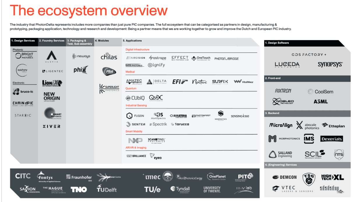
Photonics ecosystem
Step 1. Bright Photonics: the designer that makes ideas manufacturable
In the first phase of the ecosystem, everything revolves around design. Before a photonic chip can be produced, an idea must be translated into a manufacturable design with building blocks, simulations, and design rules. Bright Photonics plays exactly that role: the company helps customers design photonic integrated circuits that can later be produced in a foundry, a factory.
That puts Bright Photonics in a crucial position in the chain. Many companies that want to apply photonics do have an application or a system question, but not always the specialist knowledge required to build a PIC design from scratch. Bright Photonics lowers that threshold. Its so-called “Bright Boards” are intended to enable rapid prototyping across a wide range of applications.
That design component is important for the sector’s maturation. An ecosystem can only scale if not every project remains custom work starting from zero. Reusable building blocks, design standards, and strong support make it possible to move more quickly from idea to prototype. Bright Photonics thus shows that industrial photonics does not begin in the factory, but on the drawing board.
Step 2. SMART Photonics: the foundry as the industrial backbone
After design comes production: the factory where wafers are made. SMART Photonics is the most prominent example of a place where photonic chips are actually manufactured. For a young industry, such foundry capacity is strategic. Without production infrastructure, designs remain academic or experimental; with a foundry, a route toward scale emerges.
SMART Photonics focuses on indium phosphide, InP, an important material platform for integrated photonics, including in datacom and telecom. Especially with the rise of cloud infrastructure and AI workloads, demand for InP wafers is growing. AI requires faster and more energy-efficient optical connections, precisely the domain in which InP technology can play an important role.
SMART already has a foundry that produces 4-inch wafers for InP chips, but together with TNO, it is now working to scale up. In 2028, a foundry capable of mass production with 6-inch wafers should be available at the High Tech Campus Eindhoven. However big that step may be, SMART Photonics is already thinking hard about the next one: an even larger factory with even larger wafers and therefore even higher production volumes. So that the Netherlands becomes the place where the whole world orders its photonic chips.
Step 3. PHIX: packaging as the hidden key to scale
A chip is not yet a product. After fabrication, a PIC has to be packaged and connected to optical fibres, electronics, thermal management systems, and mechanical interfaces. That is the world of packaging, testing, and sub-assembly. In the ecosystem infographic, PHIX is positioned exactly in that phase.
Packaging may sound like a final step, but in integrated photonics, it is often one of the most difficult parts. Light must be guided into and out of the chip with extreme precision. Small deviations can have major consequences for performance, reliability, and cost. That is why packaging and sub-assembly are strategic capabilities within the value chain, not downstream activities that only become relevant at the end.
PHIX shows why the Dutch chain is relatively complete. The company helps turn photonic chips into components for customers worldwide. It is precisely here that it is determined whether photonics can make the leap from lab to factory and from prototype to product.
Step 4. Superlight Photonics: modules for ultra-broadband light
Between the chip and the end application lies the module phase. This is where photonic building blocks are integrated into usable subsystems. Superlight Photonics is one of the companies that approaches photonics as part of a functioning system.
Superlight Photonics is working on light sources based on integrated photonics. Such sources are relevant for applications that require broadband, stable, or precisely controlled light, for example, in metrology, sensing, medical imaging, or telecom. Within the logic of the ecosystem, the company therefore forms a bridge between base technology and market-specific applications.
That bridging function is becoming increasingly important. The next phase of the ecosystem will be determined by scale and adoption across multiple domains: from AI infrastructure and data communication to sensing, healthcare, and environmental monitoring. Module companies such as Superlight Photonics help translate generic photonic technology into solutions for system integrators and end customers.
Step 5. MantiSpectra: from chip to industrial sensor
The application phase shows where integrated photonics creates social and economic value. MantiSpectra is a clear example of this. The company develops spectral sensor technology at the chip level, enabling materials to be analysed quickly and compactly.
Spectral sensing can bring laboratory-like analysis into production environments, devices, and real-time processes. This allows companies to measure faster, waste less, and control quality more effectively. Integrated into a smartphone, MantiSpectra could allow a user to test immediately how fresh strawberries are or which materials are present in a product.
MantiSpectra integrates near-infrared sensing into industrial systems and develops ChipSense-based sensor modules. In doing so, MantiSpectra shows how a photonic chip only truly becomes relevant when it solves a concrete problem: measuring something that was previously too expensive, too large, or too slow to measure continuously.
Step 6. MicroAlign: precision as a condition for volume
At the back end of the ecosystem are companies that ensure chips, components, and modules can be assembled and tested accurately. MicroAlign represents a less visible but indispensable layer of the chain: precision alignment.
That precision is essential in photonics. While electronics requires electrical contacts, photonics must couple light exactly between a chip, fibre, lens, or other optical element. That requires extremely accurate positioning. As volumes increase, precision as well as reproducibility and automation become important.
Testing and back-end requirements become more complex as PICs move toward deployment. Wafer-level testing, automated optical test solutions, and system validation are needed to guarantee yield, reliability, and scalability. MicroAlign therefore symbolises a crucial lesson in deeptech: scaling is often won or lost in the details of production and assembly.
Step 7. Morphotonics: imprint technology for optical structures
Morphotonics works on nanoimprint technology: a way to reproduce extremely fine structures with high precision. In a photonic value chain, this is relevant because optical functions often depend on structures at the micro or nanoscale.
The role of such technology becomes more important as applications move closer to mass production. For displays, sensors, optical components, and other light-manipulating systems, it is not enough to build a single well-functioning prototype. The challenge is to produce the same optical performance repeatedly, affordably, and at scale.
Morphotonics thus shows another aspect of the ecosystem: the chain does not consist only of PIC companies in the strict sense. It is about a broader industry with partners in design, production, packaging, application, technology, and R&D. Specialised back-end players such as Morphotonics increase the likelihood that Dutch photonics will not only be technologically strong but also industrially viable.
The climb is getting steeper
Together, these seven companies, part of an ecosystem comprising dozens of players, show how broad the Dutch integrated photonics ecosystem has become. Bright Photonics helps to design ideas. SMART Photonics makes the chips. PHIX packages and assembles them. Superlight Photonics builds modules. MantiSpectra brings the technology into industrial sensing. MicroAlign and Morphotonics strengthen the back end needed for precision, reproducibility, and scale.
That is exactly the movement currently underway. The foundation has been laid, but the next phase will be tougher. The challenge is no longer just to show that integrated photonics works. The challenge is to grow companies, strengthen chains, and develop markets.
Although billions are currently being invested in photonics in the US and China, the Netherlands remains ahead of the competition due to the completeness of its ecosystem. Because that, too, is New Dutch: not just the factory or the application, but collaboration across the entire chain to move forward in a coherent way.
Sponsored
This story is the result of a collaboration between New Dutch and our editorial team. IO+ is an independent journalism platform that carefully chooses its partners and only cooperates with companies and institutions that share our mission: spreading the story of innovation. This way we can offer our readers valuable stories that are created according to journalistic guidelines.
Want to know more about how IO+ works with other companies? Click here